|
Shenzhen Xinchenger Electronic Co.,Ltd
|
Gold Index: 8393


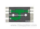
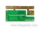
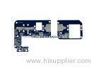
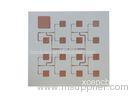
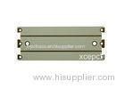
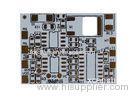
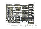
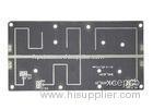
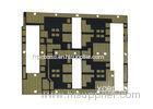
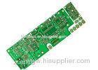
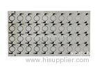
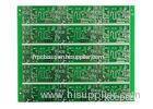
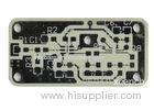
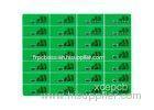
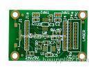
High Frequency TP-2 RF PCB Design Radio Frequency Printed Circuit Board Manufacturing
| Place of Origin: | Zhejiang, China (Mainland) |
|
|
|
| Add to My Favorites | |
| HiSupplier Escrow |
Product Detail
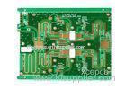
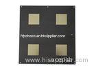
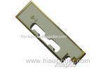
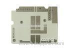
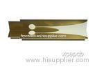
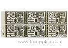
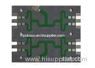
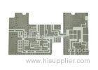
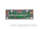
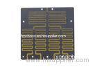
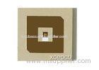
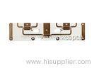
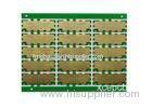
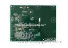
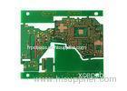
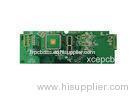
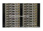
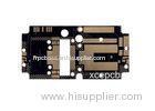
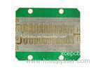
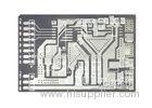
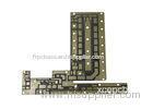
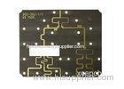
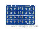
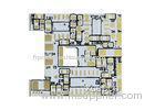
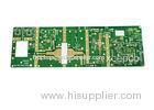
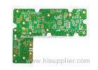
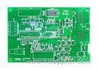
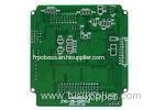
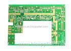
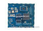
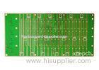
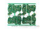
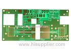
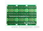
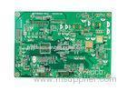
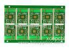
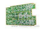
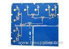
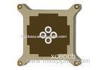
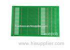
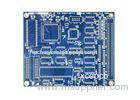
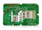
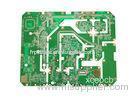
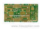
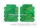
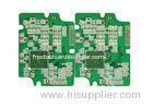
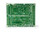
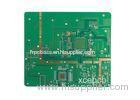
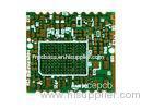
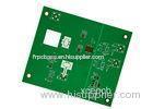
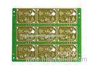
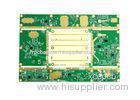
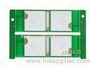
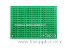
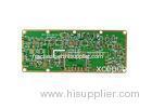
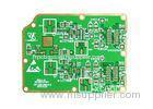
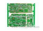
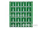
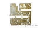
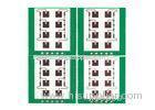
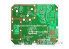
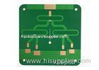
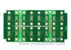
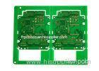
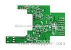
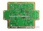
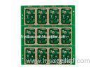
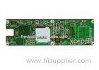
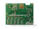
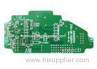
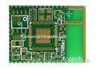
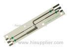
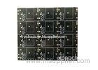
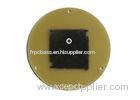
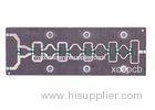
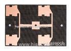
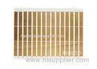
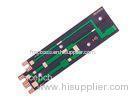
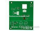
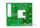
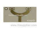
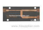
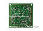
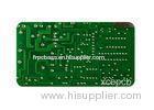
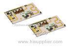
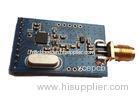
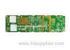
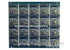
High Frequency PCB RF Design Radio Frequency Circuit Boards Fabrication
Spec
High Frequency PCB RF Design Radio Frequency Circuit Boards Fabrication
Specification:
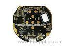
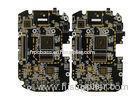
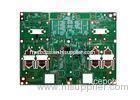
Radio frequency (RF) and microwave PCB’s are a type of PCB designed to operate on signals in the megahertz to gigahertz frequency ranges (medium frequency to extremely high frequency). These frequency ranges are used for communication signals in everything from cellphones to military radars. The materials used to construct these PCB’s are advanced composites with very specific characteristics for dielectric constant (Er), loss tangent, and CTE (co-efficient of thermal expansion).
High frequency circuit materials with a low stable Er and loss tangent allow for high speed signals to travel through the PCB with less impedance than standard FR-4 PCB materials. These materials can be mixed in the same Stack-Up for optimal performance and economics.
Parameter:
| o | Item | Data |
| 1 | Layer: | 1 to 24 layers |
| 2 | Material type: | FR-4, CEM-1, CEM-3, High TG, FR4 Halogen Free, Rogers |
| 3 | Board thickness: | 0.20mm to 3.4mm |
| 4 | Copper thickness: | 0.5 OZ to 4 OZ |
| 5 | Copper thickness in hole: | >25.0 um (>1mil) |
| 6 | Max. Board Size: | (580mm×1200mm) |
| 7 | Min. Drilled Hole Size: | 4mil(0.1mm) |
| 8 | Min. Line Width: | 3mil (0.075mm) |
| 9 | Min. Line Spacing: | 3mil (0.075mm) |
| 10 | Surface finishing: | HASL / HASL lead free, HAL, Chemical tin, Chemical Gold, Immersion Silver/Gold, OSP, Gold plating |
| 11 | Solder Mask Color: | Green/Yellow/Black/White/Red/Blue |
| 12 | Shape tolerance: | ±0.13 |
| 13 | Hole tolerance: | PTH: ±0.076 NPTH: ±0.05 |
| 14 | Package: | Inner packing: Vacuum packing / Plastic bag,Outer packing: Standard carton packing |
| 15 | Certificate: | UL,SGS,ISO 9001:2008 |
| 16 | Special requirements: | Buried and blind vias+controlled impedance +BGA |
| 17 | Profiling: | Punching, Routing, V-CUT, Beveling |
Features
- CTEr = +40/+50 ppm per °C (low); Tg (glass transition temperature) is 280°C
- ER = 3.38/3.48 at 10.0 GHz
- ER is constant to 40.0 GHz
- ED (electro-deposited) copper only
- Layer-to-layer thickness control = +/- 0.001
- Fabrication costs are typical to slightly increased
Related Search
Find more related products in following catalogs on Hisupplier.com
Related Products
Company Info
Shenzhen Xinchenger Electronic Co.,Ltd [China (Mainland)]
Business Type:Manufacturer
City: Shenzhen
Province/State: Guangdong
Country/Region: China (Mainland)